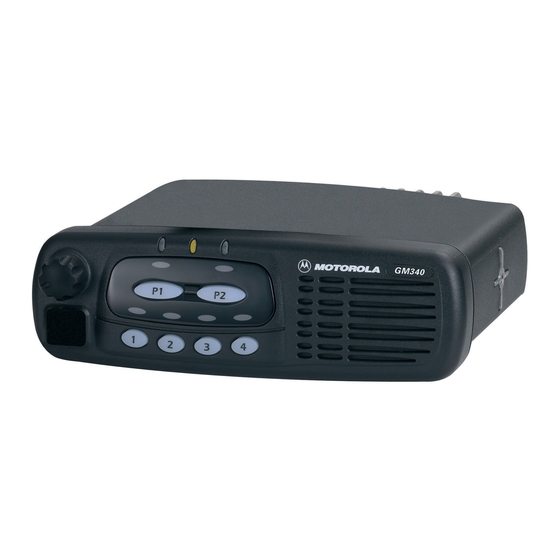
Motorola GM140 Информация о сервисе - Страница 12
Просмотреть онлайн или скачать pdf Информация о сервисе для Двухстороннее радио Motorola GM140. Motorola GM140 32 страницы. Gm series professional radio uhf (403-470mhz)
Также для Motorola GM140: Информация о сервисе (34 страниц), Базовое руководство по обслуживанию (46 страниц), Информация о сервисе (32 страниц)

2-6
3.5
Keypad Keys
The controlhead keypad is a 6-key kepad (Model B) or a 10- key keypad (model C). All keys are
configured as 2 analogue lines read by µP pins 13 and 15. The voltage on the analogue lines varies
between 0 volts and +5 volts depending on which key has been pressed. If no key is pressed, the
voltage at both lines will be 5 volts. The key configuration can be thought of as a matrix, where the
two lines represent one row and one column. Each line is connected to a resistive divider powered
by +5 volts. If a button is pressed, it will connect one specific resistor of each divider line to ground
level and thereby reduce the voltages on the analogue lines The voltages of the lines are A/D
converted inside the µP (ports PE 0 - 1) and specify the pressed button. To determine which key is
pressed, the voltage of both lines must be considered.
An additional pair of analogue lines and A/D µP ports (PE 3 – 2) is available to support a keypad
microphone, connected to the microphone connector J0811. Any microphone key press is
processed the same way as a key press on the controlhead.
3.6
Status LED and Back Light Circuit
All the indicator LED's (red, yellow, green) are driven by current sources. To change the LED status
the host radio sends a data message via SBEP bus to the controlhead µP . The controlhead µP
determines the LED status from the received message and switches the LED's on or off via port PB
7 – 0 and port PA4. The LED status is stored in the µP 's memory. The LED current is determined by
the resistor at the emitter of the respective current source transistor.
The back light for the LCD and the keypad is controlled by the host radio the same way as the
indicator LED's using µP port PA 5. This port is a Pulse Width Modulator (PWM) output. The output
signal charges capacitor C0843 through R0847. By changing the pulse width under software control,
the dc voltage of C0843 and thereby, the brightness of the back light can be changed in four steps.
The keypad back light current is drawn from the FLT A+ source and controlled by transistor Q0933.
The current flowing through the LED's cause a proportional voltage drop across the parallel resistors
R0947, R0948. This voltage drop is amplified by the op-amp U0931-2. U0931-2 and Q0934 form a
differential amplifier. The voltage difference between the base of Q0934 and the output of U0931-2
determines the current from the base of the LED control transistor Q0933 and in turn the brightness
of the LED's. The µP can control the LED's by changing the dc level at the base of Q0934. If the
base of Q0934 is at ground level, Q0934 is switched off and no current flows through Q0933 and the
LED's. If the base voltage of Q0934 rises a current flows through Q0934 and in turn through Q0933
causing the LED's to turn on and a rising voltage drop across R0947, R0948. The rising voltage
causes the output of the op-amp to rise and to reduce the base to emitter voltage of Q0934. This
decreases the current of Q0933 until the loop has settled.
3.7
Liquid Crystal Display (LCD)
The LCD H0971 uses the display driver U0971. The display is a single layer super twist nematic
(STN) LCD display. It has 14 characters with a 5*8 dot matrix for displaying alpha - numerical
information and a line with 21 pre - defined icons above the dot matrix
The driver contains a data interface to the µP, an LCD segment driver, an LCD power circuit, an
oscillator, data RAM and control logic. At power up the driver's control logic is reset by a logic „0" at
input SR2 (U0971-15). The driver's internal oscillator is set to about 20 kHz and can be measured at
pin 22. The driver's µP interface is configured to accept 8 bit parallel data input (U0971-D0-D7) from
the controlhead µP (U0831 port PC0-PC7).
To write data to the driver's RAM the µP sets chip select (U0971-20) to logic „0" via U0831-11, RD
(U0971-18) to logic „1" via (U0831-10) and WR (U0971-17) to logic „0" via U0831-9. With input A0
(U0971-21) set to logic „0" via U0831-12 the µP writes control data to the driver. Control data
THEORY OF OPERATION
