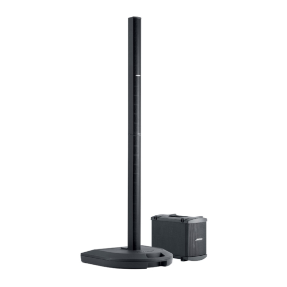
Bose Personalized Amplification System Sorun Giderme Kılavuzu - Sayfa 36
Stereo sistemi Bose Personalized Amplification System için çevrimiçi göz atın veya pdf Sorun Giderme Kılavuzu indirin. Bose Personalized Amplification System 50 sayfaları.
Ayrıca Bose Personalized Amplification System için: Kullanıcı El Kitabı (28 sayfalar)

4
3
2
1
A7
5
A6
6
A5
7
8
A4
32-lead PLCC
9
A3
Top View
10
A2
A1
11
A0
12
DQ0
13
14 15 16 17 18 19 20
29LE020 EEPROM Pinout Diagram
P
D
IN
ESCRIPTION
Sym bol
Pin Nam e
A
-A
Row Address Inputs
17
7
A
-A
Column Address Inputs
6
0
DQ
-DQ
Data Input/output
7
0
CE#
Chip Enable
OE#
Output Enable
WE#
Write Enable
V
Power Supply
DD
V
Ground
SS
NC
No Connection
F
B
UNCTIONAL
LOCK
A 17 - A 0
Address Buffer & Latches
CE#
OE#
WE#
APPENDIX
32 31 30
29
A14
28
A13
27
A8
26
A9
25
A11
24
OE#
23
A10
22
CE#
21
DQ7
Functions
To provide memory addresses. Row addresses define a page for a Write cycle.
Column Addresses are toggled to load page data
To output data during Read cycles and receive input data during Write cycles.
Data is internally latched during a Write cycle.
The outputs are in tri-state when OE# or CE# is high.
To activate the device when CE# is low.
To gate the data output buffers.
To control the Write operations.
To provide:
5.0V supply (4.5-5.5V) for SST29EE020
3.0V supply (3.0-3.6V) for SST29LE020
2.7V supply (2.7-3.6V) for SST29VE020
Unconnected pins.
29LE020 EEPROM Pinout Table
D
IAGRAM
X-Decoder
Control Logic
29LE020 EEPROM Block Diagram
1
2
-
+
3
-
+
4
TLO72, Dual Op-Amp
Y-Decoder and Page Latches
I/O Buffers and Data Latches
36
1. Output1
8
2. Inverting input1
3. Non-inverting input 1
7
4. -Vcc
5. Non-inverting input 2
6
6. Inverting input 2
7. Output 2
5
8. +Vcc
SuperFlash
Memory
DQ 7 - DQ 0
