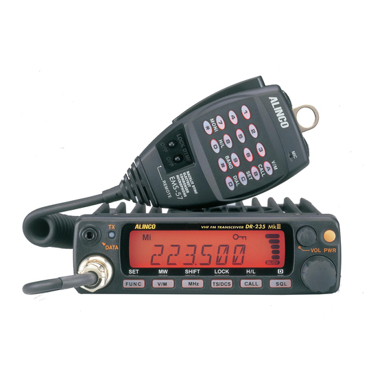
Alinco DR-235T Kullanıcı Kılavuzu - Sayfa 5
Alıcı-Verici Alinco DR-235T için çevrimiçi göz atın veya pdf Kullanıcı Kılavuzu indirin. Alinco DR-235T 10 sayfaları. Amateur mobile radio transceiver
and sounds is outputted from the speaker.)
6.AIR Band Reception
T only
If it is made air band receiving mode, IF signal is demodulated by AM decoder of IC106,and is output
from pin13 as the AF signal.
7.WIDE/NARROW switching circuit
The 2nd IF 455 kHz signal which passes through filter FL101 (wide) and FL102 (narrow) during narrow,
changes its width using the width control switching IC103 and IC102.
2) Transmitter System
1. Modulator Circuit
The audio signal is converted to an electrical signal by the microphone, and input it to the microphone
amplifier (Q6). Amplified signal which passes through mic-mute control IC109 is adjusted to an
appropriate mic-volume by means of mic-gain adjust VR106.
IC114:AandB consists of two operational amplifiers; one amplifier (pins 1, 2, and 3) is composed of pre-
emphasis and IDC circuits and the other (pins 5, 6, and 7) is composed of a splatter filter. The maximum
frequency deviation is obtained by VR107. and input to the signal switch (IC113) (9600 bps packet signal
input switch) and input to the cathode of the varicap of the VCO, to change the electric capacity in the
oscillation circuit. This produces the frequency modulation.
2. Power Amplifier Circuit
The transmitted signal is oscillated by the VCO, amplified by the drive amplifier (IC112) and younger
amplifier (Q115), and input to the final power module (IC110). The signal is then amplified by the final
power module (IC110) and led to the antenna switch (D110) and low-pass filter (L113, L114, L115, L116,
C215, C216, C202, C203 and C204), where unwanted high harmonic waves are reduced as needed, and the
resulting signal is supplied to the antenna.
3. APC Circuit
Part of the transmission power from the low-pass filter is detected by D111 and D112, converted to DC.
The detection voltage is passed through the APC circuit (Q118, Q117, Q116), then it controls the APC
voltage supplied to the younger amplifier Q115 and the final power module IC110 to fix the transmission
power.
3) PLL Synthesizer Circuit
1. PLL
The dividing ratio is obtained by sending data from the CPU (IC1) to pin 2 and sending clock pulses to pin
3 of the PLL IC (IC501). The oscillated signal from the VCO is amplified by the buffer (Q504 and Q501)
and input to pin 15 of IC501. Each programmable divider in IC501 divides the frequency of the input
signal by N according to the frequency data, to generate a comparison frequency of 5 or 6.25 kHz.
2. Reference Frequency Circuit
The reference frequency appropriate for the channel steps is obtained by dividing the 12.8 MHz reference
oscillation (X103) by 2560 or 2048, according to the data from the CPU (IC1). When the resulting
frequency is 5 kHz, channel steps of 5, 10, 15, 20, 25, 30, and 50 kHz are used. When it is 6.25 kHz, the
12.5 kHz channel step is used.
3. Phase Comparator Circuit
The PLL (IC501) uses the reference frequency, 5 or 6.25kHz. The phase comparator in the IC501