Alinx AN8238 Kullanıcı Kılavuzu - Sayfa 5
Kontrol Ünitesi Alinx AN8238 için çevrimiçi göz atın veya pdf Kullanıcı Kılavuzu indirin. Alinx AN8238 17 sayfaları. 2-channel high speed ad module

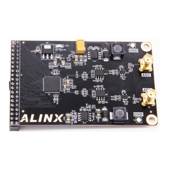
2-Channel High Speed AD Module AN9238 User Manual
Part 2: AN9238 Module Function Description
Part 2.1: AN9238 Module Hardware Block Diagram
Figure 2-1: AN9238 Module Hardware Block Diagram
For the specific reference design of the AD9238 circuit, please refer to the
AD9238 chip manual.
Part 2.1: Single-ended Input and Operational Amplifier
Circuit
The single-ended input AD1 and AD2 are input through two SMA headers,
J5 or J6, and the voltage of the single-ended input is -5V~+5V.
On the FPGA development board, the input voltage of -5V~+5V is reduced
to -1V~+1V through the AD8065 chip and voltage divider resistors. If the user
wants to input a wider range of voltage, just modify the resistance of the
front-end voltage divider resistor.
Conversion Formula: V
5/17
= (1.0/5.02)*V
OUT
IN
www.alinx.com
