Digilent chipKIT uC32 Referans Kılavuzu - Sayfa 3
Anakart Digilent chipKIT uC32 için çevrimiçi göz atın veya pdf Referans Kılavuzu indirin. Digilent chipKIT uC32 18 sayfaları.

chipKIT™ uC32™ Board Reference Manual
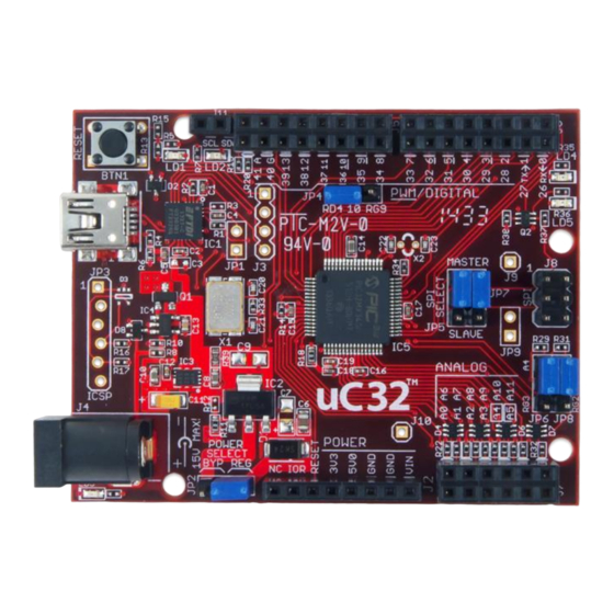
5. JP2 – Power Select Jumper
This jumper is used to route power from the external power connector through the on-board 5V
voltage regulator or to bypass the 5V regulator. The REG position routes power through the 5V
regulator. The BYP position bypasses the on-board 5V regulator. With this jumper in the BYP position
the maximum input voltage that can be applied at the external power connector is 6V.
6. Power Supply – 5V Regulator
This on-board 5V voltage regulator regulates the input voltage applied at the external power connector
to 5V. This is used to power the 3.3V regulator and to provide 5V power to expansion shields. This
regulator can provide up to 800mA of current.
7. J2 – Shield Power Connector
This connector provides power to I/O expansion shields connected to the board.
8. PIC32 Microcontroller
The PIC32MX340F512H microcontroller is the main processor for the board.
9. J7 – Analog Signal Connector
This connector provides access to analog/digital I/O pins on the microcontroller.
10. JP6/JP8 – A4/A5 Signal Select Jumpers
These jumpers are used to switch pins 9 and 11 on connector J7 between analog inputs A4 and A5 or
2
the I
C signals SDA and SCL.
11. J8 – SPI Signal Connector
This connector provides alternative access to the SPI signals. This is used by some shields for access to
the SPI bus.
12. JP5/JP7 – SPI Master/Slave Select Jumpers
These jumpers are used to switch the SPI signals for use of the uC32 board as an SPI master device or as
an SPI slave device. Both jumpers should be switched together. Place the shorting blocks in the MASTER
position for master operation and in the SLAVE position for slave operation. Normally, these jumpers
are in the MASTER position.
13. User LEDs
Two LEDs connected to digital signal pins 13 and 43.
14. J6 – Digital Signal Connector
This connector provides access to digital I/O pins on the microcontroller.
15. JP4 – Pin 10 Signal Select Jumper
This jumper is used to switch connector J5 pin 5 (digital signal 10) between pulse width modulator
(PWM) operation and SPI operation. The jumper is placed in the RD4 position for PWM output and in
the RG9 position for SPI slave operation. The shorting block on this jumper will normally be in the RD4
position. The only time it normally needs to be in the RG9 is when using the Uno32 board as an SPI
slave device.
16. J5 – Digital Signal Connector
This connector provides access to digital I/O pins on the microcontroller.
2
17. J11 – I
C
2
Dedicated I
C signals. These pins are independent of the settings of jumpers JP6 and JP8. However, if
JP6 and JP8 are in the RG3 and RG2 position, the I
Copyright Digilent, Inc. All rights reserved.
Other product and company names mentioned may be trademarks of their respective owners.
2
C signals will be tied to pins A4 and A5 on J7.
Page 3 of 17
