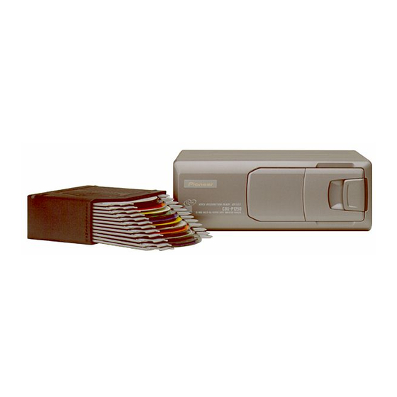
Pioneer CDX-P1250 Servis Kılavuzu - Sayfa 35
CD Çalar Pioneer CDX-P1250 için çevrimiçi göz atın veya pdf Servis Kılavuzu indirin. Pioneer CDX-P1250 50 sayfaları. Multi-compact disc player

7. GENERAL INFORMATION
7.1 IC
- Pin Functions (UPD63710GC)
Pin No.
Pin Name
1
GND
2
HOLD
3
MIRR
4
FOK
rst
5
6
A0
stb
7
sck
8
9
SO
10
SI
11
VDD
12
DA.VDD
13
NC
14, 15
DA.GND
16
NC
17
DA.VDD
18
R+
19
R-
20
L-
21
L+
22
X.VDD
xtal
23
24
XTAL
25
X.GND
26
VDD
27
EMPH
28
FLAG
29
DIN
30
DOUT
31
SCKIN
32
SCKO
33
LRCKIN
34
LRCK
35
WDCK
36
TX
37
GND
38
C16M
39
LIMIT
40
VDD
41
LOCK
42
RFCK
43
WFCK
44
PLCK
45
GND
46
C1D1
47
C1D2
48
C2D1
49
C2D2
50
C2D3
51
VDD
I/O
Function and Operation
Logic circuit GND
I/O
Defect detection output
I/O
MIRR output
O
RFOK signal output
I
Reset signal input
I
Command/parameter identification signal input
I
Data strobe signal input
I
Clock signal input for serial data input/output
O
Serial data and status signal output
I
Serial data input
Positive power supply terminal to logic circuit
Positive power supply terminal to D/A converter
Not used
D/A converter GND
Not used
Positive power supply terminal to D/A converter
O
Right channel audio data output
O
Right channel audio data output
O
Left channel audio data output
O
Left channel audio data output
Positive power supply terminal to crystal oscillation circuit
O
Crystal oscillator connect pin
I
Crystal oscillator connect pin
Crystal oscillation circuit GND
Positive power supply terminal to logic circuit
O
Output pin for the pre-emphasis data in the sub-Q code
O
Flag output pin to indicate that audio data currently being output consists
of noncorrectable data
I
Serial data input to internal DAC
O
Serial audio data output
I
Serial clock input to internal DAC
O
Audio data that is output from DOUT changes at rising edge of this clock
I
LRCK signal input to internal DAC
O
Signals to distinguish the right and left channels of the audio data output
from DOUT
O
Output double the frequency of LRCK
O
Digital audio interface data output
Logic circuit GND
O
Oscillator clock buffering output
I
Status of the pin is output at Bit 5 of the status output
Positive power supply terminal to logic circuit
O
EFM synchronous detection signal
O
Frame synchronous signal of XTAL-system
O
Frame synchronous signal of PLL-system
O
Monitor pin of bit clock
Logic circuit GND
O
Output pin for indicating the C1 error correction results
O
Output pin for indicating the C1 error correction results
O
Output pin for indicating the C2 error correction results
O
Output pin for indicating the C2 error correction results
O
Output pin for indicating the C2 error correction results
Positive power supply terminal to logic circuit
CDX-P1250
35
