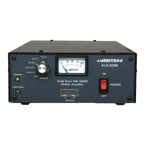
AMERITRON ALS-500MXCE Інструкція з експлуатації - Сторінка 3
Переглянути онлайн або завантажити pdf Інструкція з експлуатації для Підсилювач AMERITRON ALS-500MXCE. AMERITRON ALS-500MXCE 19 сторінок.

ALS-500M
Instruction Manual
GENERAL INFORMATION
Load Fault Circuit
The ALS-500M features a load fault trip circuit that bypasses the amplifier if the amplifier frequency
switch is set to a lower frequency range than the exciter or if the load reflected power exceeds 70-100
watts. This circuit virtually eliminates the danger of component failures due to operating errors.
The Combiner circuit board near the PA contains the components that sense the reflected power at the
input of the low-pass filters used in the output circuit. Selecting a filter that has a cut off frequency
below the operating frequency or operating into loads with reflected power levels that exceed 70-100
watts will trip the overload and bypass the amplifier. SCR (Q5) on the Bias board keeps the amplifier
"locked out" until the POWER (ON/OFF) switch is cycled off and on.
Bias Control Circuits
The Bias board contains the temperature and bias control circuitry. The output transistor temperature is
monitored with diodes D1 and D2 on the PA module. The voltage drop across the diodes decreases as
the PA transistor temperature rises. The reduction in diode voltage with increasing temperature causes
IC 1c/d to reduce the PA base bias current supplied by Q2/3. Diodes D1/2 on the bias board limit the
available bias voltage if a failure in the bias circuit occurs.
IC 1a compares the voltage from the Power Amplifier temperature diodes to the reference voltage from
the temperature sensitivity control R28. If the temperature becomes too high (voltage too low) IC 1a
switches high and Q4 turns the cooling fan on. If the temperature continues to increase IC 1b will
eventually pull low and the voltage for the transmit relay and the bias voltage will be removed. The
THERMAL OVERLOAD LED is illuminated when the output of IC 1b is low. This circuit
automatically resets when the temperature drops to a safe operating range.
If the band switch is in the wrong position, the antenna SWR is high, or the amplifier is being driven
into non-linear operation a "load fault" will occur. When a load fault occurs gate voltage is applied to
SCR Q5. This causes Q5 to latch in a conducting state. Q5 will remain in this condition and the
amplifier's relay line will be disabled until the OFF/ON switch is cycled off and on. The LOAD
FAULT LED on the front panel is illuminated whenever SCR Q5 is in conduction and the amplifier is
bypassed from a load fault.
Drive Power
The ALS-500M normally requires much less than 100 watts of drive to produce full output power.
This drive power varies considerably with the gain of the transistors used in the amplifier and the
power supply voltage. As a general rule, exceeding 100 watts of drive for long periods of time may
cause component failures. Exceeding 70 watts of peak drive power may cause distortion and increase
the bandwidth of the transmitted signal.
2
