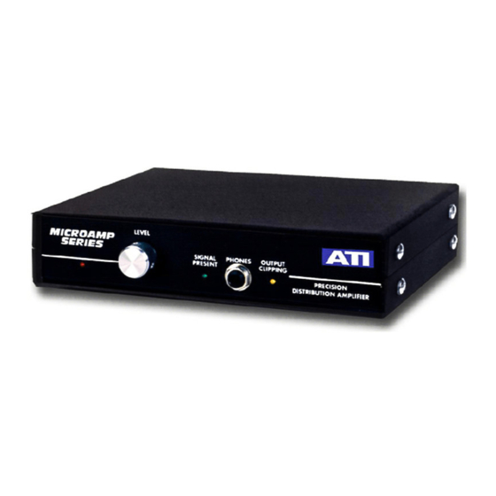
ATI Technologies DA1000 Посібник з експлуатації та технічного обслуговування - Сторінка 3
Переглянути онлайн або завантажити pdf Посібник з експлуатації та технічного обслуговування для Підсилювач ATI Technologies DA1000. ATI Technologies DA1000 6 сторінок. Ati distribution amplifier operating and maintenance manual

OUTPUTS
Audio from the input buffer is AC coupled to the front panel level adjusts potentiometer.
This control adjusts the level of all outputs. If you are afflicted with lurking knob
twiddlers, the knob can be removed leaving a somewhat less inviting screwdriver
adjustment. If removing the knob doesn't cure the problem, put your DA out of reach by
sticking it to the ceiling using the supplied suction cup feet.
The pot output is applied to the non-inverting input of the HI (in-phase) output stage
driver IC (A2-1). The IC supplies the first 10 mA of output current directly and then the
complementary Class B output booster transistors (Q1 and Q2) take over. The unique,
wide bandwidth, high slew rate circuit design provides effective class AB operation with
minimal crossover distortion from a power output stage operating true Class B with zero
quiescent power dissipation.
The HI output bus is applied to the inverting input of A2-2 in a unity gain, phase
inverting configuration and boosted by Q3 and Q4 to form the LO output bus.
The HI and LO output buses are split into nine individual outputs (eight rear and one
front panel jack) through 150 ohm build out resistances. All outputs will tolerate short
circuits across the output or to ground without damage. Up to two outputs can be shorted
with no significant reduction in headroom. Needless to say, this is NOT the
recommended mode of operation - do not drive single ended (one side grounded) loads
from both HI and LO outputs together. Drive single ended loads from either the HI or LO
outputs to ground. Up to 18 single ended 600-ohm output loads may be simultaneously
driven.
The build-out resistors are split and heavily bypassed to prevent RIF pickup on the output
lines from affecting operation of the DA. These bypasses will place a very heavy load on
the outputs under sustained sine wave operation above 20kHz and such operation may
over dissipate the 47 ohm build-out resistors - don't do it!
OUTPUT CLIPPING INDICATOR
The differential input voltage of H1 output driver IC (A2-1) is monitored by A3. The
differential voltage is under a few millivolts under linear operation, however, if the
output is driven to clipping, the differential voltage rapidly increases and is amplified to
light the yellow OUTPUT CLIPPING LED. Conserve power - try not to light the yellow
LED.
HEADPHONE OUTPUT
The front panel headphone jack provides a ninth output with its own set of build out
resistors. The phone jack is a convenient metering point, an auxiliary output or
headphone output. The jack is wired primarily to drive stereo headphones with an inphase
mono signal consequently tip (red) and ring (blue) are wired together and to the HI output
Day Sequerra │ 154 Cooper Rd. #902 │ W. Berlin, NJ 08091 │ Voice 856-719-9900 │ [email protected] │ www.atiaudio.com
