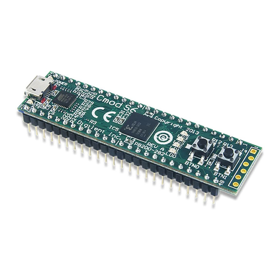
Digilent Cmod S6 Довідковий посібник - Сторінка 4
Переглянути онлайн або завантажити pdf Довідковий посібник для Материнська плата Digilent Cmod S6. Digilent Cmod S6 5 сторінок. Fpga board

Cmod S6™ FPGA Board Reference Manual
Address (HEX
value)
0 (0x0)
1 (0x1)
2 (0x2)
3 (0x3)
4 (0x4)
5 (0x5)
6 (0x6)
7 (0x7)
8 (0x8)
9 (0x9)
10 (0xA)
11 (0xB)
The least significant bit in any register corresponds to the smallest pin number that it controls. Registers 6 through
11 will set up a pin controlled by registers 0 through 5 as an input if the corresponding bit in the register is a logic
'1' and will set up the pin as an output if the corresponding bit in the register is a logic '0'. For example, if the value
stored in register 6 is 11110000 in binary (0xF0 in HEX), the pins 1-4 on the Cmod S6 will be set as outputs and pins
5-8 will be set as inputs. When a pin is configured as an output, it will initially be driven low (logic '0').
The source code for this project can be found on the Cmod S6 product page of the Digilent website,
www.digilentinc.com.
Copyright Digilent, Inc. All rights reserved.
Other product and company names mentioned may be trademarks of their respective owners.
Function
Stores the logic value present on pins 1 through 8
Stores the logic value present on pins 9 through 16
Stores the logic value present on pins 17 through 23
Stores the logic value present on pins 26 through 33
Stores the logic value present on pins 34 through 41
Stores the logic value present on pins 42 through 48
Controls the I/O state of pins 1 through 8
Controls the I/O state of pins 9 through 16
Controls the I/O state of pins 17 through 23
Controls the I/O state of pins 26 through 33
Controls the I/O state of pins 34 through 41
Controls the I/O state of pins 42 through 48
Table 1. DEPP Register Map for factory loaded configuration.
Page 4 of 4
