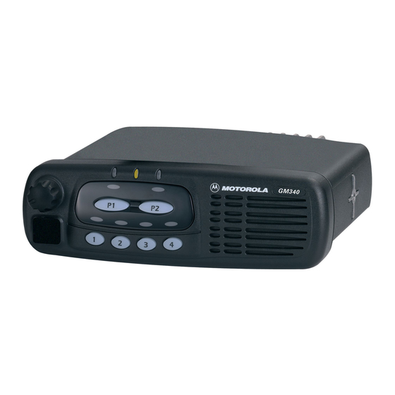
Motorola GM Series Сервісна інформація - Сторінка 19
Переглянути онлайн або завантажити pdf Сервісна інформація для Радіо Motorola GM Series. Motorola GM Series 34 сторінки. Professional radio
Також для Motorola GM Series: Посібник з експлуатації (28 сторінок), Посібник з монтажу (36 сторінок)

VHF (136-174MHz) Transmitter Power Amplifier (PA) 45 W
signal into a digital code that is applied to the loop divider, thereby causing the carrier to deviate. The
balance attenuator is used to adjust the VCO's deviation sensitivity to high frequency modulating
signals. The output of the balance attenuator is present at the MODOUT port (U3201-41) and
connected to the VCO modulation diode D3362 via R3364.
5.0
VHF (136-174MHz) Transmitter Power Amplifier (PA) 45 W
The radio's 45 W PA is a four stage amplifier used to amplify the output from the VCOBIC to the
radio transmit level. The line-up consists of three stages which utilize LDMOS technology, followed
by a final stage using a bipolar device. The gain of the first stage (U3401) is adjustable, controlled by
pin 4 of PCIC (U3501) via Q3501 and Q3502 (VCONT). It is followed by an LDMOS pre-driver stage
(Q3421), an LDMOS driver stage (Q3431) and a bipolar final stage (Q3441).
From VCO
Controlled
Stage
Vcontrol
To Microprocessor
Devices U3401 and Q3421 are surface mounted. The remaining devices are directly attached to the
heat sink.
5.1
Power Controlled Stage
The first stage (U3401) is a 20dB gain integrated circuit containing two LDMOS FET amplifier
stages. It amplifies the RF signal from the VCO (TXINJ). The output power of stage U3401 is
controlled by a DC voltage applied to pin 1 from the power control circuit (U3501 pin 4, with
transistors Q3501 and Q3502 providing current gain and level-shifting). The control voltage
simultaneously varies the bias of two FET stages within U3401. This biasing point determines the
overall gain of U3401 and therefore its output drive level to Q3421, which in turn controls the output
power of the PA.
In receive mode the voltage control line is at ground level and turns off Q3501-2, which in turn
switches off the biasing voltage to U3401.
Pre
PA
PA-Final
Driver
Driver
Stage
Bias 2
A S F I C _ C M P
SPI BUS
Bias 1
Figure 2-1 VHF Transmitter Block Diagram
Pin Diode
Antenna
Switch
Power
Sense
PA
PWR
SET
P C I C
To Microprocessor
Antenna
Harmonic
Filter
RF Jack
Temperature
Sense
To Microprocessor
2-9
