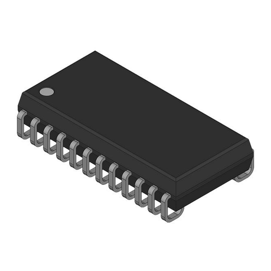
Cypress Semiconductor CY7C1306BV25 Технічна специфікація - Сторінка 13
Переглянути онлайн або завантажити pdf Технічна специфікація для Комп'ютерне обладнання Cypress Semiconductor CY7C1306BV25. Cypress Semiconductor CY7C1306BV25 20 сторінок. Cypress 18-mbit burst of 2 pipelined sram with qdr architecture specification sheet

Scan Register Sizes
Register Name
Instruction
Bypass
ID
Boundary Scan
Instruction Codes
Instruction
EXTEST
IDCODE
SAMPLE Z
RESERVED
SAMPLE/PRELOAD
RESERVED
RESERVED
BYPASS
Document #: 38-05627 Rev. *A
Bit Size
3
1
32
107
Code
000
Captures the Input/Output ring contents.
001
Loads the ID register with the vendor ID code and places the register
between TDI and TDO. This operation does not affect SRAM operation.
010
Captures the Input/Output contents. Places the boundary scan register
between TDI and TDO. Forces all SRAM output drivers to a High-Z state.
011
Do Not Use: This instruction is reserved for future use.
100
Captures the Input/Output ring contents. Places the boundary scan register
between TDI and TDO. Does not affect the SRAM operation.
101
Do Not Use: This instruction is reserved for future use.
110
Do Not Use: This instruction is reserved for future use.
111
Places the bypass register between TDI and TDO. This operation does not
affect SRAM operation.
CY7C1303BV25
CY7C1306BV25
Description
Page 13 of 19
[+] Feedback
