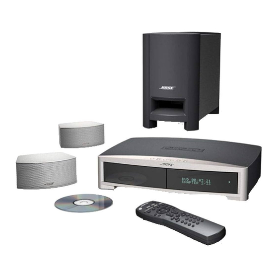
Bose 3-2-1 Handbuch zur Fehlersuche - Seite 21
Blättern Sie online oder laden Sie pdf Handbuch zur Fehlersuche für Home Theater System Bose 3-2-1 herunter. Bose 3-2-1 28 Seiten. Home entertainment system
Auch für Bose 3-2-1: Benutzerhandbuch (44 seiten), Handbuch zur Schnelleinrichtung (1 seiten)

•
•
2.2 3
2
1 Series II Bass Module Details
The bass module contains all the active audio processing and amplification electronics of the
•
•
3
2
1 Series II System. The rear end cap of the bass module provides access to the following
components:
•
Line cord socket
•
Power Switch (European only)
•
System Connector (13-pin)
•
Array Speaker Connector (DB9-S)
All the above components are mounted on the I/O Printed Circuit Assembly, part number
270926-001, which is, in turn, secured to the end cap via a metal bracket. The dash suffix is
used to denote the various AC voltage variants.
All other electronics reside on the DSP/Amplifier PCB Assembly. The DSP/Amp PCB is secured
to the extruded aluminum heat sink (which is glued to the back baffle of the module enclosure)
with a metal bracket. This bracket provides sufficient compression force to the PCB to maintain
good thermal contact to the heat sink of the audio power amplifiers, rectifier diodes, and pre-
regulator FET.
The power transformer for the system is directly mounted to the end baffle of the module above
the heat sink.
2.2.1 I/O Printed Circuit Assembly
Note: Refer to the Input/Output (I/O) PCB schematic diagram, 270926, for the following infor-
mation.
The I/O printed circuit assembly contains the AC input connector J1 [C4], the line switch S1 [D3]
and line fuse F1 [C3]. Connector J2/J5 [D2], depending on the dash (-xxx) variation, provides
the primary power connection to the power transformer. A location for a MOV (VR1 [C3]) is
provided, but is not populated in production.
Connectors J6 [B7] and J7 [D8] connect the I/O PCB to the DSP PCB. J6 connects to a 16-
position ribbon cable which carries the S/PDIF and audio inputs and control signals to/from the
DSP board. J7 connects to a 10-position cable that brings the array speaker amplifier outputs
and Vunreg/GND onto the I/O PCB. C7-9 provide RF ground coupling between the various
ground pins and structures on the board. C1, C3, C4, C5, and C10 are DC blocking caps on
the differential audio inputs and associated GND. C6 is the bulk storage capacitor for the
Vunreg supply. All of the signals described in section 3.1 are connected to the 13-pin system
connector J3 [B2] on this board.
2.2.2 DSP/Amplifier Printed Circuit Assembly
This board provides the following major functions:
Note: Refer to the DSP/Amplifier PCB schematic diagrams, 270921, for the following informa-
tion.
THEORY OF OPERATION
21
