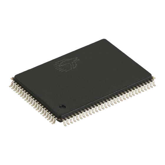
Cypress Semiconductor CY7C1339G Spezifikationsblatt - Seite 3
Blättern Sie online oder laden Sie pdf Spezifikationsblatt für Computer Hardware Cypress Semiconductor CY7C1339G herunter. Cypress Semiconductor CY7C1339G 18 Seiten. Cypress 4-mbit (128k x 32) pipelined sync sram specification sheet

Pin Configurations
(continued)
M
Pin Definitions
Name
I/O
A
, A
, A
Input-
0
1
Synchronous
BW
, BW
Input-
A
B
BW
, BW
Synchronous
C
D
GW
Input-
Synchronous
BWE
Input-
Synchronous
CLK
Input-
Clock
CE
Input-
1
Synchronous
CE
Input-
2
Synchronous
CE
Input-
3
Synchronous
OE
Input-
Asynchronous
Document #: 38-05520 Rev. *F
119-Ball BGA Pinout
1
2
A
V
A
DDQ
NC/288M
CE
B
2
C
NC/144M
A
DQ
NC
D
C
E
DQ
DQ
C
C
F
V
DQ
DDQ
C
DQ
DQ
BW
G
C
C
H
DQ
DQ
C
C
J
V
V
DDQ
DD
K
DQ
DQ
D
D
L
DQ
DQ
BW
D
D
V
DQ
DDQ
D
N
DQ
DQ
D
D
P
DQ
NC
D
R
NC
A
MODE
T
NC
NC/72M
U
V
NC
DDQ
Address Inputs used to select one of the 128K address locations. Sampled at the rising edge
of the CLK if ADSP or ADSC is active LOW, and CE
are fed to the two-bit counter. .
Byte Write Select Inputs, active LOW. Qualified with BWE to conduct byte writes to the SRAM.
Sampled on the rising edge of CLK.
Global Write Enable Input, active LOW. When asserted LOW on the rising edge of CLK, a global
write is conducted (ALL bytes are written, regardless of the values on BW
Byte Write Enable Input, active LOW. Sampled on the rising edge of CLK. This signal must be
asserted LOW to conduct a byte write.
Clock Input. Used to capture all synchronous inputs to the device. Also used to increment the
burst counter when ADV is asserted LOW, during a burst operation.
Chip Enable 1 Input, active LOW. Sampled on the rising edge of CLK. Used in conjunction with
CE
and CE
to select/deselect the device. ADSP is ignored if CE
2
3
when a new external address is loaded.
Chip Enable 2 Input, active HIGH. Sampled on the rising edge of CLK. Used in conjunction with
CE
and CE
to select/deselect the device.CE
1
3
loaded.
Chip Enable 3 Input, active LOW. Sampled on the rising edge of CLK. Used in conjunction with
CE
and CE
to select/deselect the device. CE
1
2
loaded. Not connected for BGA. Where referenced, CE
document for BGA.
Output Enable, asynchronous input, active LOW. Controls the direction of the I/O pins. When
LOW, the I/O pins behave as outputs. When deasserted HIGH, I/O pins are tri-stated, and act as
input data pins. OE is masked during the first clock of a read cycle when emerging from a
deselected state.
3
4
5
A
A
ADSP
A
A
ADSC
A
V
A
DD
V
NC
V
SS
SS
V
CE
V
SS
1
SS
V
OE
V
SS
SS
ADV
BW
c
B
V
GW
V
SS
SS
NC
V
NC
DD
V
CLK
V
SS
SS
NC
BW
D
A
V
V
BWE
SS
SS
V
A1
V
SS
SS
V
A0
V
SS
SS
V
NC
DD
A
A
A
NC
NC
NC
Description
, CE
1
is sampled only when a new external address is
2
is sampled only when a new external address is
3
3
CY7C1339G
6
7
A
V
DDQ
NC/9M
NC/576M
A
NC/1G
NC
DQ
B
DQ
DQ
B
B
DQ
V
B
DDQ
DQ
DQ
B
B
DQ
DQ
B
B
V
V
DD
DDQ
DQ
DQ
A
A
DQ
DQ
A
A
DQ
V
A
DDQ
DQ
DQ
A
A
NC
DQ
A
A
NC
NC/36M
ZZ
NC
V
DDQ
, and CE
are sampled active. A1, A0
2
3
and BWE).
[A:D]
is HIGH. CE
is sampled only
1
1
is assumed active throughout this
Page 3 of 18
[+] Feedback
