Bose Personalized Amplification System Manual de solución de problemas - Página 20
Navegue en línea o descargue pdf Manual de solución de problemas para Sistema estéreo Bose Personalized Amplification System. Bose Personalized Amplification System 50 páginas.
También para Bose Personalized Amplification System: Manual del usuario (28 páginas)

THEORY OF OPERATION
1.5.8 Digital to Analog Converter (Analog)
The stereo D/A converter U387 [B5] is of type Crystal CS4392. It has two symmetrical outputs
that get turned into an unbalanced signal through difference amplifier U388A [D7] /U388B [B7].
These OpAmp sections also form additional 2-pole low-pass filters that help remove out-of-band
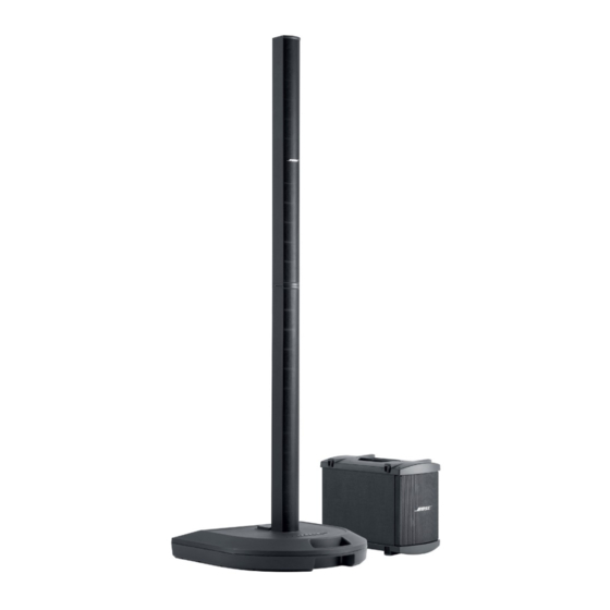
components from the audio output. The "left" output contains the signal for L1 Cylindrical Radia-
tor™ loudspeaker and the "right" output contains the signal for the B1 bass module. These get
routed through CN115 back to the input panel board.
1.5.9 Power Amp Inputs and Bass Line Out
J113 Bass Line Out jack [input panel PCB sheet 2, D3] provides a TRS balanced & buffered
version of the "right" / bass output from the D/A. This is used primarily for driving another PS1,
which in turn powers 2-6 additional B1 Bass Modules (see 1.3.1 figure 10, "Heavy Bass" con-
figuration). Both + and – signals are resistor-isolated so that either balanced or unbalanced ¼"
phone connections may be used.
An "All-Amps-In" connector J112 [C1] allows a single input to drive all 3 amplifiers equally. This
will most often be driven from the Bass Line Out of another PS1 as mentioned above. J112's
switching configuration allows both high and low frequency channels to drive the appropriate
channels when the All-Amps-In connector isn't in use, and allows the addition of a buffer U112A
[B3] to maintain a greater than 10k ohm input impedance when the connector is used.
J114, 115 and 116 [C/D4] allow each power amplifier to be driven separately; this would gener-
ally only be used in special applications where a single "slave" PS1 is used to add bass from two
different "master" PS1's.
1.5.10 Power Amplifiers
Note: Refer to the Digital Amplifier PCB schematic sheets for the following information.
Each of the PS1's 3 amplifier channels is implemented with a 2-chip Class-D solution from
Philips. The three identical channels are located on one PCB assembly, but they are kept
independent by separate power supply, I/O and control connections. Each TDA8929T PWM
controller (U803, U806 and U809) [sheets 2, 3 and 4, C4] interfaces directly to two TDA8927J
(U801, U802, U804, U805, U807 and U808) power output stages. Normally, only one 8927 is
used, but in our case, the two halves of each 8927 are operated in parallel (doubling the avail-
able output current), and the two paralleled chips are driven out of phase to achieve the bridged
output configuration. Current sharing between the two halves of the 8927 chips is achieved by a
separate output LC filter for each section. The direct interface allows excess current in any one
of the output stages to immediately shut down all drive signals from the 8929 controller chip.
Numerous bypassing and filtering elements are added to the power amplifier to mitigate the
effects of the high currents at the nominal switching frequency of about 300 kHz.
In addition to the overcurrent shutdown path (amp shuts down power supply), there is other
outboard circuitry added to shut down an amplifier channel if the corresponding power supply
voltage is too low (usually due to extreme overdrive), and also another path to shut down a
channel's power amp and power supply if excess DC voltage appears at the output.
20
