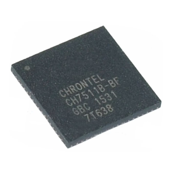
Chrontel CH7511B Manual de diseño - Página 6
Navegue en línea o descargue pdf Manual de diseño para Receptor Chrontel CH7511B. Chrontel CH7511B 16 páginas. Edp/dp receiver

CHRONTEL
• AUXP and AUXN
These two pins are for Display Port AUX channel control that accepts a half-duplex, bi-directional AC-coupled
differential signal. An AC coupling capacitor, 0.1uF recommended, must be placed on the end as shown in Figure 6.
• HPDET
This output pin indicates whether the device is active or not. It also generates an interrupt pulse as defined by the
Display Port standard. Output voltage is 3.3V. A resistor, greater than 100KΩ, should be connected between this pin
and GND as shown in Figure 6.
2.6
LVDS Signal Pins
• LVDS Outputs (LDCxP and LDCxN)
The LVDS output signals are LDCxP and LDCxN. The LVDS is a differential interface with a nominal swing 200mV.
The following rules should be applied to the signals:
1.
Keep traces as short as possible.
Make these traces have 100Ω differential impedance.
2.
3.
Trace widths should be 5 mils.
Intra Pair spacing (spacing between the "+" and "-" pairs) should be 7mils.
4.
5.
Inter Pair spacing (spacing between one differential pair and another) should be a minimum of 20 mils
except in the area near the pins.
Difference in trace lengths between "+" and "-" pairs should be within 5mils.
6.
7.
Difference in trace lengths among Inter pairs should be within 10mils.
"+" And "-" pairs should be routed in parallel.
8.
2.7
Other function pins
6
Figure 5: CH7511B/7512B DP Main Link Lane Inputs
U1
43
AU XN
44
AU XP
59
HP DET
R1
100 K
CH 7511B
Sink
R5
R6
1M
1M
U3
43
C5 0.1 uF
AU XN
44
C6 0.1 uF
AU XP
59
HP DET
R3
100 K
CH 7512B
Sink
Figure 6: CH7511B/7512B AUX channel and HPDET
U2
C1 0.1 uF
AU XN
C2 0.1 uF
AU XP
HP DET
R2
100 K
GMCH
Source eDP
+3. 3V
+3. 3V
R7
R8
100 K
100 K
C3 0.1 uF
AU XN
C4 0.1 uF
AU XP
HP DET
R4
100 K
Source DP
206-1000-014
AN-B014
U4
GMCH
Rev. 1.7
2020-07-14
