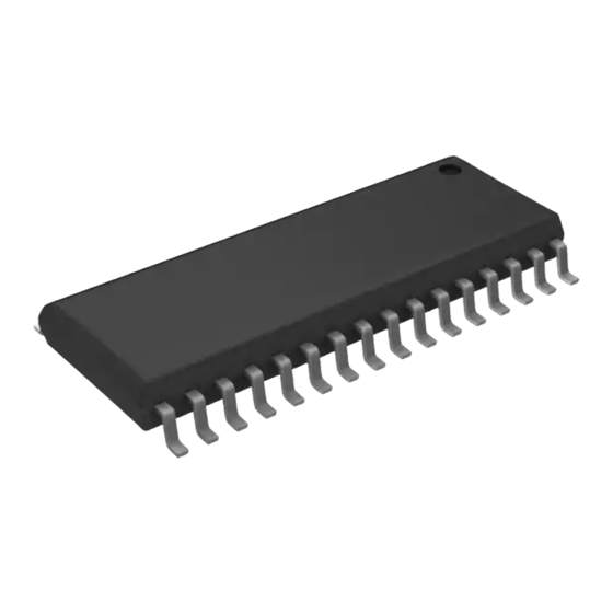
Cypress Semiconductor CY62148E Fiche technique
Parcourez en ligne ou téléchargez le pdf Fiche technique pour {nom_de_la_catégorie} Cypress Semiconductor CY62148E. Cypress Semiconductor CY62148E 11 pages. Mobl 4-mbit (512k x 8) static ram

Features
• Very high speed: 45 ns
• Voltage range: 4.5V–5.5V
• Pin compatible with CY62148B
• Ultra low standby power
— Typical standby current: 1 µA
— Maximum standby current: 7 µA (Industrial)
• Ultra low active power
— Typical active current: 2.0 mA @ f = 1 MHz
• Easy memory expansion with CE, and OE features
• Automatic power down when deselected
• CMOS for optimum speed and power
• Available in Pb-free 32-pin TSOP II and 32-pin SOIC
packages
Product Portfolio
Product
Range
CY62148ELL
TSOP II
CY62148ELL
SOIC
Ind'l/Auto-A
Notes
1. For best practice recommendations, refer to the Cypress application note "System Design Guidelines" at http://www.cypress.com.
2. SOIC package is available only in 55 ns speed bin.
3. Typical values are included for reference only and are not guaranteed or tested. Typical values are measured at V
Cypress Semiconductor Corporation
Document #: 38-05442 Rev. *F
[2]
V
Range (V)
CC
[3]
Min
Typ
Ind'l
4.5
5.0
4.5
5.0
•
198 Champion Court
4-Mbit (512K x 8) Static RAM
Functional Description
The CY62148E is a high performance CMOS static RAM
organized as 512K words by 8 bits. This device features
advanced circuit design to provide ultra low active current.
This is ideal for providing More Battery Life™ (MoBL
portable applications such as cellular telephones. The device
also has an automatic power down feature that significantly
reduces power consumption when addresses are not toggling.
Placing the device into standby mode reduces power
consumption by more than 99% when deselected (CE HIGH).
The eight input and output pins (IO
in a high impedance state when:
• Deselected (CE HIGH)
• Outputs are disabled (OE HIGH)
• Write operation is active (CE LOW and WE LOW)
To write to the device, take Chip Enable (CE) and Write Enable
(WE) inputs LOW. Data on the eight IO pins (IO
is then written into the location specified on the address pins
(A
through A
).
0
18
To read from the device, take Chip Enable (CE) and Output
Enable (OE) LOW while forcing Write Enable (WE) HIGH.
Under these conditions, the contents of the memory location
specified by the address pins appear on the IO pins.
Speed
Operating I
(ns)
f = 1MHz
[3]
Max
Typ
Max
5.5
45
2
2.5
5.5
55
2
2.5
,
•
San Jose
CA 95134-1709
CY62148E MoBL
[1]
through IO
) are placed
0
7
through IO
0
Power Dissipation
(mA)
CC
Standby I
SB2
f = f
max
[3]
[3]
Typ
Max
Typ
Max
15
20
1
15
20
1
= V
, T
= 25°C.
CC
CC(typ)
A
•
408-943-2600
Revised March 28, 2007
®
®
) in
)
7
(µA)
7
7
[+] Feedback
