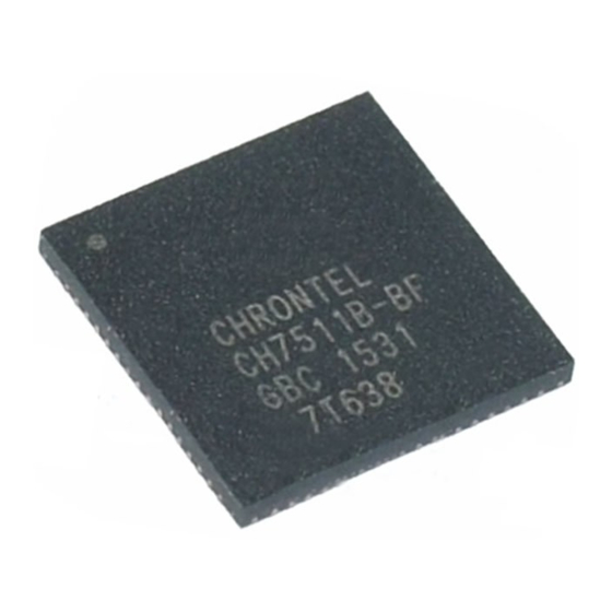
Chrontel CH7511B Podręcznik projektowania
Przeglądaj online lub pobierz pdf Podręcznik projektowania dla Odbiornik Chrontel CH7511B. Chrontel CH7511B 16 stron. Edp/dp receiver

Chrontel
PCB Layout and Design Guide for CH7511B and CH7512B
I
1.0
NTRODUCTION
Chrontel's CH7511B/7512B is an eDP/DP receiver that integrates LVDS Transmitter for the notebook/AIO display.
The CH7511B is designed to comply with the Embedded Display Port Specification 1.2 and the CH7512B is
designed to comply with the Display Port Specification 1.1a. The CH7511B/7512B provides support for two main
link lanes with data rate running at either 1.62Gb/s or 2.7Gb/s, and accepts data in 18-bit 6:6:6 or 24-bit 8:8:8 RGB
digital format. During system power-up, setting the power on/off sequence for a particular panel can be achieved
through the CH9904 Boot ROM registers. The CH7511B/7512B has incorporated a brightness control function to
interface with LCD backlight module. Brightness control commands sent through AUX Channel are dynamically
translated by the CH7511B/7512B and converted into the LCD backlight control signals.
The CH7511B/7512B can support 18-bit Single Port, 18-bit Dual Port, 24-bit Single Port and 24-bit Dual Port LVDS
outputs in both OpenLDI and SPWG bit mapping for LVDS application. The CH7511B/7512B supports LVDS
output up to 1920x1200.
This application note focuses only on the basic PCB layout and design guidelines for the CH7511B/7512B eDP/DP
Receiver with LVDS Transmitter. Guidelines in component placement, power supply decoupling, grounding, input
/output signal interface are discussed in this document.
The discussion and figures presented in this document are based on the 68-pin QFN (8x8 mm) package of the
CH7511B/7512B. Please refer to the CH7511B/7512B datasheet for details of the pin assignments.
2.0
C
OMPONENT
Components associated with the CH7511B/7512B should be placed as close as possible to the respective pins. The
following will describe guidelines on how to connect critical pins, as well as the guidelines for the placement and
layout of components associated with these pins.
2.1
Power Supply Decoupling
The optimal power supply decoupling is accomplished by placing a 0.1μF ceramic capacitor at each of the power
supply pins as shown in Figure 1. These capacitors (C1, C2, C3, C4, C5, C7, C8, C10, C11, and C12) should be
connected as close as possible to their respective power and ground pins using short and wide traces to minimize lead
inductance. Whenever possible, a physical connecting trace should connect the ground pins of the decoupling
capacitors to the CH7511B/7512B ground pins, in addition to ground vias.
2.1.1
Ground Pins
The CH7511B/7512B should be connected to a common ground plane to provide a low impedance return path for the
supply currents. Whenever possible, each of the CH7511B/7512B ground pins should be connected to its respective
decoupling capacitor ground lead directly, and then connected to the ground plane through a ground via. Short and
wide traces should be used to minimize the lead inductance. Refer to Table 1 for the Ground pin assignments.
206-1000-014
Rev. 1.7
P
LACEMENT AND
2020-07-14
D
C
ESIGN
ONSIDERATIONS
AN-B014
Application Note
1
