Avnet ROHM Semiconductor Руководство пользователя - Страница 5
Просмотреть онлайн или скачать pdf Руководство пользователя для Блок управления Avnet ROHM Semiconductor. Avnet ROHM Semiconductor 8 страниц. Power module

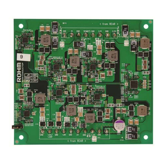
J3 (Samtec part # FW-05-05-F-D-361-085) is in place to provide access for remote voltage
sense. The mating connector on the baseboard is Samtec part # CLP-105-02-F-D. The signals
on this header are tied directly to the load voltage pins. This header is pinned out left to right
down the header as illustrated below:
Pins are defined as follows:
Pin 1 location on J3 is indicated on the silk screen on the PCB. Pin 1 on J1 and J2 are the right
most pins when viewing the board header side up. Refer to Figure 2 for an illustration of these
pin positions.
2.3 DDR Memory Voltage Select Jumper
JP3 sets the output of the 1.5V / 1.35V regulator. JP1 is a 2 pin header with a jumper selected
to be open or closed. Place the jumper on pins 1-2 to set the voltage to 1.5V. Leave the jumper
open to set the voltage to 1.35V. The table below shows the jumper settings and corresponding
output voltage.
Setting the voltage to 1.5V or 1.35V is dependent on the type of memory utilized on the target
board. In the case of the K7 Mini-Module for example, the DDR memory used is 1.5V.
WARNING:
Be sure to check that the voltage is set to the proper level before powering the
board. Using the wrong voltage can cause damage to the device or the target board.
Copyright © 2012 Avnet, Inc. AVNET and the AV logo are registered trademarks of Avnet, Inc. All other brands are property of their respective owners.
Avnet Electronics Marketing
Pin
2
Signal
2.5Vrm
1Vmgtrm
Pin
1
Signal
3.3Vrm
JP1 setting
Open
Closed
Table 6 – JP3 Jumper Settings
1
2
3
4
5
6
7
8
9
10
Table 4 - J3 Diagram
4
6
2Vrm
3
5
1.8Vrm
1Vrm
Table 5 - J3 Pinout
Output voltage
1.35V
1.5V
5 of 8
8
10
1.2Vrm
GND
7
9
1.5Vrm
GND
Rev A 1.0
06/05/2013
