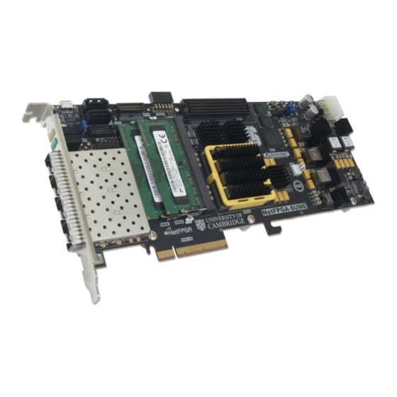
Digilent NetFPGA-SUME Довідковий посібник - Сторінка 13
Переглянути онлайн або завантажити pdf Довідковий посібник для Материнська плата Digilent NetFPGA-SUME. Digilent NetFPGA-SUME 20 сторінок.

NetFPGA-SUME™ Reference Manual
The following sections provide greater detail about programming the NetFPGA-SUME using the different methods
available.
3.1
JTAG Configuration
The Xilinx tools typically communicate with FPGAs using the Test Access Port and Boundary-Scan Architecture,
commonly referred to as JTAG. During JTAG programming, a .bit file is transferred from the PC to the FPGA using
the onboard Digilent USB-JTAG circuitry (port J16) or an external JTAG programmer, such as the Digilent JTAG-HS2,
attached to port J9. You can perform JTAG programming any time after the NetFPGA-SUME has been powered on,
regardless of whether or not the mode jumper (JP1) is set. If the FPGA is already configured, then the existing
configuration is overwritten with the bitstream being transmitted over JTAG. Setting the mode jumper is useful to
prevent the FPGA from being configured from the parallel flash.
Programming the NetFPGA-SUME with an uncompressed bitstream using the on-board USB-JTAG circuitry usually
takes around a minute. JTAG programming can be done using the hardware server in Vivado or the iMPACT tool
included with ISE.
3.2
Configuration using Parallel Flash
In order to meet the PCIe specification, an expansion card must be able to respond to PCI enumeration commands
within 200 milliseconds of the power supplies becoming stable. On the NetFPGA-SUME, responding to PCI
commands requires the FPGA to be configured, so meeting this spec requires an extremely fast configuration
solution be used. This is achieved by using a CPLD that reads a stored bitstream out of flash and configures the
FPGA over a 32-bit SelectMAP interface clocked at 100MHz.
Digilent designed the firmware for the CPLD so that four different bitstreams can be stored in the flash. On power-
up (if JP1 is not loaded), one of these bitstreams is read by the CPLD and used to program the FPGA. The bitstream
that is used is determined by a non-volatile register called the "Boot Section Select" (BSS) register. If the BSS
register points to a section that does not contain a valid bitstream, the Error LED (LD5) is illuminated and the FPGA
is not configured.
After the FPGA has been programmed (whether by JTAG or from parallel flash), it is possible for the design to
trigger the CPLD to reconfigure the FPGA with one of the stored bitstreams. This is done by selecting the desired
bitstream with the CPLD_IMGSEL0 and CPLD_IMGSEL1 pins and then driving CPLD_RECONFIG high. For example, if
CPLD_IMGSEL0='0' and CPLD_IMGSEL1='1' when CPLD_RECONFIG is driven high, the FPGA will immediately be
reprogrammed with the bitstream stored in boot section 2. If the boot section indicated by the CPLD_IMGSEL pins
does not contain a valid bitstream, then the bitstream in the section pointed to by the BSS register is used and the
Fallback LED (LD6) is illuminated. Note that the CPLD_IMGSEL2 pin is not used.
After the CPLD has successfully programmed the FPGA, the boot section that the bitstream was loaded from is
indicated using the IMGCUR0 (LD7) and IMGCUR1 (LD8) LEDs. The IMGCUR2 LED (LD9) is not used.
Bitstreams are programmed into or read from flash using the dsumecfg tool included with the Adept Utilities
package. You can also use this tool to set the BSS register. The Adept Utilities toolset can be downloaded for free
from the Adept 2 page on the
installation. The following should be kept in mind when using the dsumecfg tool:
In order to use dsumecfg, you must have the NetFPGA-SUME connected to your computer via the USB-
JTAG port.
To decrease programming times, we highly recommend enabling bitstream compression in Vivado or ISE
when you generate your bitstream.
Copyright Digilent, Inc. All rights reserved.
Other product and company names mentioned may be trademarks of their respective owners.
Digilent
website. Full documentation on the dsumecfg tool is included with the
Page 13 of 18
