Gan Systems GS-EVB-HBDB-IMS Manuale tecnico - Pagina 4
Sfoglia online o scarica il pdf Manuale tecnico per Scheda madre Gan Systems GS-EVB-HBDB-IMS. Gan Systems GS-EVB-HBDB-IMS 20. 650 v universal half bridge isolated driver motherboard for ims2 & ims3
GS-EVB-HBDB-IMS
650 V Universal Half Bridge Isolated Driver Motherboard for IMS2
& IMS3
Technical Manual
____________________________________________________________________________________________________________________________________________
List of Figures
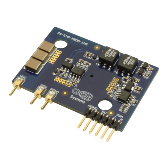
Figure 1 IMS EVB motherboard GS-EVB-HBDB-IMS .......................................................................................... 6
Figure 2 Assembled IMS EVB module with heatsink ............................................................................................ 6
Figure 3 Circuit block diagram of IMS EVB Module ............................................................................................ 7
Figure 4 Labelled driver motherboard.................................................................................................................... 7
Figure 5 Gate driver circuit (Silicon Labs P/N: Si8271) ......................................................................................... 8
Figure 6 External 5V and PWM signals connector pin ......................................................................................... 8
Figure 7 Soldering pin guide .................................................................................................................................... 9
Figure 8 Cross-section view of IMS assembly showing the power loop path ................................................. 10
Figure 9 Compatible IMS2 daughter power boards ........................................................................................... 10
Figure 10 Compatible IMS3 daughter power boards ......................................................................................... 11
Figure 11 GS66516B and GS66508B GaNPX® packaged GaN E-mode transistor .......................................... 11
Figure 12 Cross-section view of a single layer IMS board ................................................................................. 11
Figure 13 Double pulse test setup schematics ..................................................................................................... 12
Figure 14 Double pulse test setup ......................................................................................................................... 13
Figure 15 Double pulse test waveforms (400V/30A) ........................................................................................... 13
Figure 16 Boost configuration test setup schematics .......................................................................................... 14
Figure 17 Boost configuration test setup .............................................................................................................. 14
Figure 18 Boost configuration test thermal measurement result ...................................................................... 15
Figure 19 Test waveforms (400Vin, 10kHz, Po=0.8kW) ...................................................................................... 15
List of Tables
Table 1 GS-EVB-IMS3-665xxB-GS Evaluation Kit Contents ................................................................................. 5
Table 2 Compatible IMS daughter power board for driver motherboard GS-EVB-HBDB-IMS .................... 10
Table 3 Part numbers and description ................................................................................................................... 12
GS-EVB-HBDB-IMS TM Rev. 220329
© 2022 GaN Systems Inc.
www.gansystems.com
4
Please refer to the Evaluation Board/Kit Important Notice on page 19